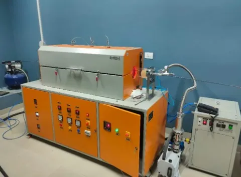
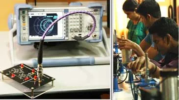
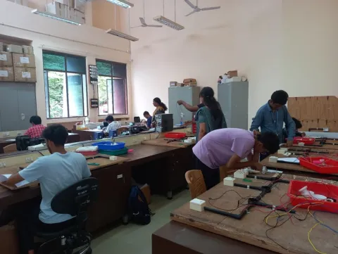
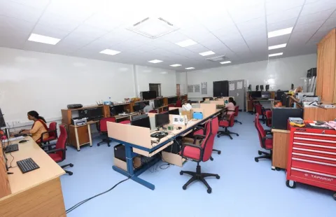
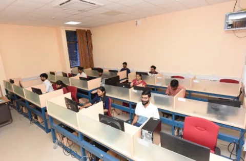
The laboratories/research facilities are established under Department of Avionics Engineering. Various experimental setups are developed in these labs to crater to the need of undergraduate and post graduate programs. In addition, several research facilities are also developed to support the research activities under the Department

Power Electronics Research Lab
-
Image
The Power Electronics Laboratory of the Avionics Department is well-equipped for performing basic as well as advanced experiments in Power Electronics and Drives. Equipment and devices required for conducting experiments on open-loop and closed-loop control of AC-DC, DC-DC, DC-AC, and AC-AC converters are available in this laboratory. In addition, facilities are available for performing advanced experiments on DC drives, 3-phase AC drives, multiphase AC drives (split phase and 5-phase), photovoltaic systems, solid-state transformers, microgrids, and more. The control schemes are implemented in custom-built digital platforms such as FPGAs, Digital Signal Controllers, and Microcontrollers.
Some of the equipment includes:
- Electronic Loads - 4 Channels up to 600V/60A
- DC power supplies - 60V/38 Amps
- Solar Array Simulator – Agilent E4360A
- dSPACE Advanced Control Education Kit
- 8-channel mixed signal oscilloscope with voltage and current probes - Yokogawa
- Motor control trainers - FEEDBACK
- Five-phase open-end winding induction motors
- Six-phase (split phase) open-end winding induction motors (10 kW)
- Six-phase wound rotor open-end winding synchronous motors (3 kW)
- DC dynamometers (13 kW)
- Configurable inverter modules (600 VDC, 75 Amps)


Research Laboratories for MEMS, Microelectronics Design, Fabrication, and Characterization
-
Image
-
Image
-
Image
Research in the area of Microsystems/Microelectronics (Semiconductor device and technology) demands good in-house design, fabrication and characterization labs. The following three major laboratories for design, fabrication and characterization with funding from IIST as well through sponsored research projects have been established. With this our PG and research students could get hands –on experience in device development.
These research labs have helped in supporting an R&D ecosystem in Microelectromechanical Systems (MEMS)/ Micro/Nano electronics and sensors at IIST.
In addition to collaborations with academia, we also have collaborations with ISRO centres like IISU, SCL etc. IIST is one of the “Collaborating institutes” with CeNSE IISc for MeitY’s INUP Idea to Innovation program.
The laboratories and research facilities would eventually evolve to an R&D Centre for NEMS & Opto/Nanoelectronics (NEMO) to promote research and technology development activities in the following area.
1. NEMS & Microelectronics Characterization and Sensor Systems Laboratories
- NEMS & Microelectronics characterization and NEMS Sensor Systems laboratories have been established with characterization/testing equipments with funding support from institute and research projects.
- Experimental setups established for Electrical characterization (I-V, C-V, etc. ) of Micro/Nanoelectronics devices, NEMS/MEMS using DC Probe station, semiconductor analyzers, SMUs,Digital Multimeter, DSO etc.
- Experimental setups established for Mechanical and electromechanical Characterization thin films, MEMS/NEMS devices VLSI and NEMS sensor systems- Nanoindentation, Microsystem Analyzer, Laser Doppler Vibrometry (LDV), Electrodynamic shaker, semiautomatic force tester/4-point /3-point bending test setup etc.
- Customized experimental setups for electromechanical characterization of MEMS nanomechanical sensors, sensor testing setup for gas and environmental sensing using nanomechanical sensors etc.
2. VLSI & Microsystems Design Lab
Microsystems design facility is equipped with modelling, design and simulation tools for MEMS devices, Micro/Nanoelectronics devices and systems. (High end workstations, Coventorware and MEMS+ from Coventor, Sentaures TCAD 3D Process and Device TCAD from Synopsis, COMSOL Multiphysics etc.)
3. MEMS an NanoFAB (Microfabrication laboratory)-Phase I
MEMS/Micro/nanofabrication facility is for 4” silicon wafer substrates with upgradability for 6” wafers. Phase-1 of MEMS & NanoFAB has been established with the major equipment’s for MEMS and microfabrication processes with funding support from institute and research projects. Deposition tools-DC/RF/Pulse DC sputtering, ICPCVD, Parylene CVD Photolithography-Double Side Mask aligner, Oxygen Plasma RIE, Anneal Tools-2D material anneal furnace, vacuum anneal etc., and Class-1000 cleanroom are part of this Phase -I

RF and Microwave Lab
-
Image
RF and Microwave Lab of the department is equipped with various facilities to perform both classical and modern experiments. Apart from Waveguide test-bench based experiments, facilities like transmission line trainer kit, antenna radiation pattern measurement set up, characterization of microwave network and antennas using spectrum and network analyzer are existing in this lab. The lab is also equipped with various advanced electromagnetic CAD softwares like HFSS, CST, Feko, ADS etc. extremely useful for state of the art research in this domain.
Major facilities of this lab includes:
- Microwave Test Bench Set-up
- Transmission Line Trainer Kit
- Spectrum Analyzer
- Vector Network Analyzer
- Microwave Signal Generator
- Antenna Measurement Set-up
- EM Simulator: HFSS, CST, FEKO, ADS
- PCB Prototyping Machine

Soldering and Wiring Lab
-
Image
The Soldering and Wiring Lab provides hands-on training to B.Tech students in essential electronics skills, focusing on soldering techniques, wire harnessing, and circuit assembly. Students are trained to solder various types of components on PCB to build functional circuits. Basic training on designing and implementation of an electrical power distribution system, covering different aspects like the selection of components, sizing of conductors etc. is imparted in this lab. In general, this lab equips the students with practical knowledge required for building reliable electronic systems used in engineering projects.

Systems and Networks Lab
-
Image
The Systems and Networks Lab (SysNet Lab) at the Department of Avionics, Indian Institute of Space Science and Technology, is a research laboratory specializing in networked systems as well as next-generation computer networks. The lab’s key research areas include Mobile Ad-hoc Networks (MANETs), Wireless Mesh Networks (WMNs), Wireless Sensor Networks (WSNs), Delay Tolerant Networks (DTNs), Software Defined Networks (SDNs), Internet of Things (IoT), satellite networking, Satellite Edge Computing (SEC), 5G/6G satellite integration, 5G/6G testbed development, CubeSat development, Space-Based Hosting Service (SBHS), quantum computing, Brain-Computer Interface (BCI), complex networks, and graph signal processing..
5G/6G Satellite Experiments
The 5G testbed is based on the SrSRAN and Open5GS framework and focuses on the development and integration of 5G/6G technologies. Further, simulation testbed enables experimentation with low-latency communications, as well as testing satellite-terrestrial network integration, handover, and edge computing capabilities.
Brain-Computer Interface (BCI) testbed
The BCI testbed creates BCI datasets for various Indian languages, utilizing OpenBCI hardware. These datasets are used for research in multilingual BCI systems and the development of machine learning and deep learning algorithms that recognize and process brain signals for neuromuscular disorders.
Space-Based Hosting Service (SBHS) hardware and software testbed
The SBHS testbeds provide a platform for deploying and testing databases on satellite and high-altitude balloon platforms. This enables researchers to explore novel architectures and communication protocols for space-based hosting services and edge computing services for remote and rural regions of the world.
Wireless Mesh Network testbed
Additionally, the lab has set up the Wireless Mesh Network (WMN) testbed, "IIST MeshNet," covering D2 and D4, to study the behavior of wireless multihop networks. SDN capabilities have been integrated into the mesh routers for granular network control and enhanced performance analysis.
The lab is equipped with a variety of hardware and software tools, including:
Hardware
- SrSRAN-based 5G testbed
- OpenBCI board-based BCI testbed
- CubeSat/balloon-based SBHS testbed
- Wireless Sensor Network testbeds and platforms
- Wireless Mesh Network testbeds
- Software Defined Network testbed
- Alix3d3 board-based wireless mesh routers
- Inforce IFC 6410 board-based wireless router platform
- Raspberry Pi boards
- Intel Galileo GEN 2 for IoT applications
- IRIS motes and sensors
Software
- NetSim Simulator
- Matlab, Simulink, KiCad
- Wireless Sensor Network testbeds and platforms
- Satellite network simulator
- Network Simulator Software (e.g., Ns-2, Ns-3, GloMoSim, Stanford Enhanced GloMoSim, OMNET++)
- Sensor Simulator Software (e.g., MoteView, MoteConfig, TinyOS)
- Mesh Network Simulator Software (e.g., Voyage Linux OS, MadWiFi Driver, OLSR/DSR/AODV routing protocols)
- Urban Delay Tolerant Network Simulator (UDTNSim v0.1), developed in-house for DTN simulations.

VLSI Design Lab
-
Image
This lab was established to support the Post Graduate program VLSI and Microsystems introduced in the year 2013 and research activities in the areas of VLSI. Modelling, design and simulation tools for MEMS devices, Micro/Nanoelectronics devices and systems. (High end workstations, Coventorware and MEMS+ from Coventor, Silvaco ATLAS and ATHENA TCAD,Sentaures TCAD 3D Process and Device TCAD from Synopsis,COMSOL Multiphysics etc.)
Major equipments
Analog and Digital IC design Tools from Cadence, Synopsys, Mentor Graphics, FPGA design tools and boards, MEMS software, TCAD software, Logic Analyzer, High end PCs.