Research Laboratories for MEMS, Microelectronics Design, Fabrication, and Characterization
Research in the area of Microsystems/Microelectronics (Semiconductor device and technology) demands good in-house design, fabrication and characterization labs. The following three major laboratories for design, fabrication and characterization with funding from IIST as well through sponsored research projects have been established. With this our PG and research students could get hands –on experience in device development.
These research labs have helped in supporting an R&D ecosystem in Microelectromechanical Systems (MEMS)/ Micro/Nano electronics and sensors at IIST.
In addition to collaborations with academia, we also have collaborations with ISRO centres like IISU, SCL etc. IIST is one of the “Collaborating institutes” with CeNSE IISc for MeitY’s INUP Idea to Innovation program.
The laboratories and research facilities would eventually evolve to an R&D Centre for NEMS & Opto/Nanoelectronics (NEMO) to promote research and technology development activities in the following area.
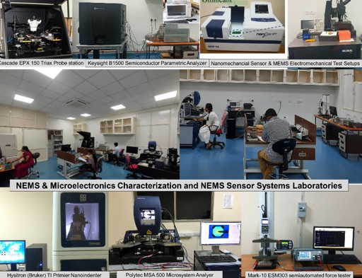
1. NEMS & Microelectronics Characterization and Sensor Systems Laboratories
- NEMS & Microelectronics characterization and NEMS Sensor Systems laboratories have been established with characterization/testing equipments with funding support from institute and research projects.
- Experimental setups established for Electrical characterization (I-V, C-V, etc. ) of Micro/Nanoelectronics devices, NEMS/MEMS using DC Probe station, semiconductor analyzers, SMUs,Digital Multimeter, DSO etc.
- Experimental setups established for Mechanical and electromechanical Characterization thin films, MEMS/NEMS devices VLSI and NEMS sensor systems- Nanoindentation, Microsystem Analyzer, Laser Doppler Vibrometry (LDV), Electrodynamic shaker, semiautomatic force tester/4-point /3-point bending test setup etc.
- Customized experimental setups for electromechanical characterization of MEMS nanomechanical sensors, sensor testing setup for gas and environmental sensing using nanomechanical sensors etc.
2. VLSI & Microsystems Design Lab
Microsystems design facility is equipped with modelling, design and simulation tools for MEMS devices, Micro/Nanoelectronics devices and systems. (High end workstations, Coventorware and MEMS+ from Coventor, Sentaures TCAD 3D Process and Device TCAD from Synopsis, COMSOL Multiphysics etc.)
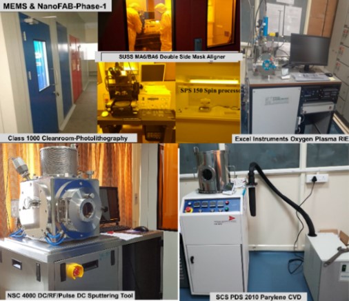
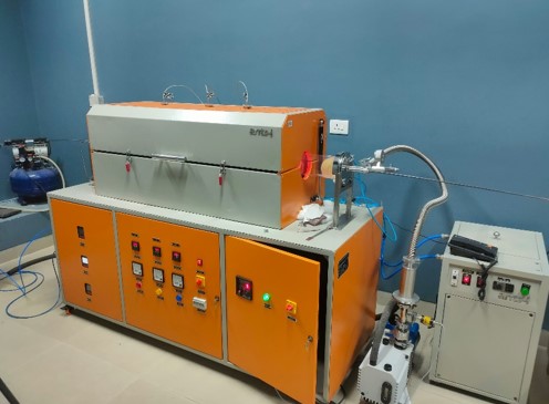
3. MEMS an NanoFAB (Microfabrication laboratory)-Phase I
MEMS/Micro/nanofabrication facility is for 4” silicon wafer substrates with upgradability for 6” wafers. Phase-1 of MEMS & NanoFAB has been established with the major equipment’s for MEMS and microfabrication processes with funding support from institute and research projects. Deposition tools-DC/RF/Pulse DC sputtering, ICPCVD, Parylene CVD Photolithography-Double Side Mask aligner, Oxygen Plasma RIE, Anneal Tools-2D material anneal furnace, vacuum anneal etc., and Class-1000 cleanroom are part of this Phase -I